






03 Sept 2026
VSP-P1 NanoPrinter
.jpg)
 (1) - Edited.jpg)
VSParticle provides an integrated set of R&D tools for generating highly pure nanoparticles and depositing nanoporous thin films with control over composition and morphology, and path toward commercial scale-up.
VSP-G1 Nanoparticle Generator
- Technology: Spark ablation (clean, dry, solvent-free nanoparticle production process)
- Materials: 40+ compatible elements, most conductive materials, i.e. metals, or (highly) doped semiconductors, carbon, as well as alloys.
- Particle size: ~ 2- 20 nm1 (material and settings dependent)
- Purity: 100% pure particles, no solvents, no surfactants, no contamination
- Output: Stable dry aerosol (typical particle concentration 108-1010 particles/cm³)
- Operating conditions: Room temperature and ambient pressure
VSP-P1 NanoPrinter
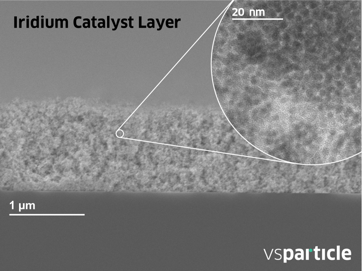
- Function: Controlled deposition of nanoparticles into porous thin films and layers
- Materials: Any conductive or properly doped semiconductive materials, alloys or combinations (40+ compatible materials, ratio-controlled mixing*)
- Material compositions tested (Multi G1 setup): >5002
- Customizable material loading: Thicknesses from several tens of nm to several µm
- Flexibility in substrate type and size: Silicon wafers (up to 6”), Nafion, Ti PTL (up to 15 x 15cm, larger substrates per request), MEMS devices ITO glass, polymers, and other types of common substrates
- Mask-less and dry fabrication
- Binder-free process: solvent-free; no ionomers or chemical precursors
- Layer thickness: Depends on the application, wide range from 10nm-10μm. Uniform and adjustable thickness
- Porosity 3(%): 50-80%
- Deposition mode: Uniform coatings or patterned deposition via XYZ stage
Deposition Services
VSParticle manufactures custom nanoporous layers directly on customer substrates, enabling rapid material combination, validation and testing for different application fields.
Capabilities
- Materials: 40+ (conductive) elements, alloys and nanoparticulate mixtures thereof
- Layer structure & morphology:
- Porosity: from compacted layers to high surface area open structures
- Thickness: from disperse distribution of nanoparticles up to several micron thick layers
- Flexible substrate type and size: Nafion, Silicon wafer, Ti PTL, and other substrates of choice up to 15 x 15cm, larger substrates per request.